 HANSUN
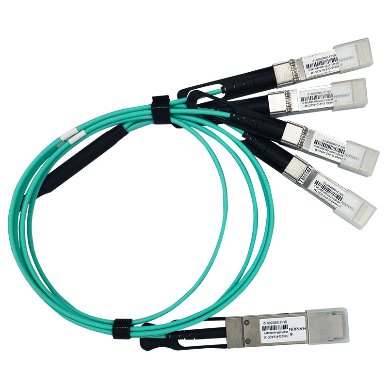

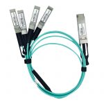
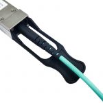
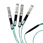
HANSUN Communication HX40-Q-410-A0CxM is a Four-Channel, Pluggable, Parallel, Fiber-Optic QSFP+SR4 for 40 Gigabit Ethernet Applications. This transceiver is a high-performance module for short-range multi-lane data communication and interconnect applications. It integrates four data lanes in each direction with 40 Gbps bandwidth. Each lane can operate at 10Gbps up to 300 m using OM3 fiber. As a professional AOC factory in China, HANSUN mainly designs these modules to operate over multimode fiber systems using a nominal wavelength of 850nm. The electrical interface uses a 38 contact edge type connector. The optical interface uses a 12 fiber MTP (MPO) connector.
Applications of 100G QSFP28 AOC
- 40GbE and 10GbE break-out applications for Datacom switch and router connections
- 40G to 4×10G density applications for Datacom and Proprietary protocol applications, Datacenters
Specifications of 40G QSFP+Breakout AOC
Absolute Maximum Ratings
| Parameter | Symbol | Min | Max | Unit |
| Storage Temperature | HX | -20 | 85 | ℃ |
| Relative Humidity | RH | 0 | 85 | % |
| Case Operating Temperature | TCase | 0 | 70 | ℃ |
| Supply Voltage | VCC | -0.5 | 3.6 | V |
Recommended Operating Conditions
| Parameter | Symbol | Min | Typical | Max | Unit |
| Case Operating Temperature | TCase | 0 | 70 | ℃ | |
| Supply Voltage | VCC | 3.13 | 3.3 | 3.47 | V |
| Supply Current (QSFP+) | ICC | 300 | mA | ||
| Supply Current(SFP+) | ICC | 100 | mA | ||
| Data Rate Per Lane | DR | 10.3125 | Gbit/s |
Electrical Characteristics
Measurement condition: Channel data rate 10.3125Gbps, VCC=3.3V, PRBS31 pattern, Case operating temperature 0-70℃
| Parameter | Symbol | Min | Typical | Max | Unit |
| QSFP+ | |||||
| Center wavelength | λc | 840 | 850 | 860 | nm |
| Differential Input Impedance | Zin | 80 | 100 | 120 | Ohm |
| Differential Input Voltage | Vin | 120 | 1600 | mVp-p | |
| Average Launch Power per Lane | PAVG | -5 | -1 | +1 | dBm |
| Extinct Ratio | ER | 3.0 | dB | ||
| SFP+ | |||||
| Center wavelength | λc | 840 | 850 | 860 | nm |
| Differential Input Impedance | Zin | 90 | 100 | 110 | Ohm |
| Differential Input Voltage | Vin | 200 | 1600 | mVp-p | |
| Average Launch Power | PAVG | -6.5 | 0 | dBm | |
| Extinct Ratio | ER | 3.0 | dB | ||
| Parameter | Symbol | Min | Typical | Max | Unit |
| QSFP+ | |||||
| Center wavelength | λc | 840 | 850 | 860 | nm |
| Differential Input Impedance | Zin | 80 | 100 | 120 | Ohm |
| Differential Input Voltage | Vin | 120 | 1600 | mVp-p | |
| Average Launch Power per Lane | PAVG | -5 | -1 | +1 | dBm |
| Extinct Ratio | ER | 3.0 | dB | ||
| SFP+ | |||||
| Center wavelength | λc | 840 | 850 | 860 | nm |
| Differential Input Impedance | Zin | 90 | 100 | 110 | Ohm |
| Differential Input Voltage | Vin | 200 | 1600 | mVp-p | |
| Average Launch Power | PAVG | -6.5 | 0 | dBm | |
| Extinct Ratio | ER | 3.0 | dB |
Receiver Specifications
| Parameter | Symbol | Min | Typical | Max | Unit |
| QSFP+ | |||||
| Center wavelength | λc | 840 | 850 | 860 | nm |
| Differential Output Impedance | Zout | 80 | 100 | 120 | Ohm |
| Differential Output Voltage | Vout | 320 | 450 | mVp-p | |
| Receiver Sensitivity | SEN | -12 | -10 | dBm | |
| Bit Error Rate | BER | 10-12 | |||
| SFP+ | |||||
| Center wavelength | λc | 840 | 850 | 860 | nm |
| Differential Output Impedance | Zout | 90 | 100 | 110 | Ohm |
| Differential Output Voltage | Vout | 370 | 1600 | mVp-p | |
| Receiver Sensitivity | SEN | -10 | dBm | ||
| Bit Error Rate | BER | 10-12 |
 - 1")
 - 3")
 - 1")


